


United Kingdom (EN)
Select your region or country.


Simulation technology | OEM camera solutions
Optimal camera selection with minimal effort
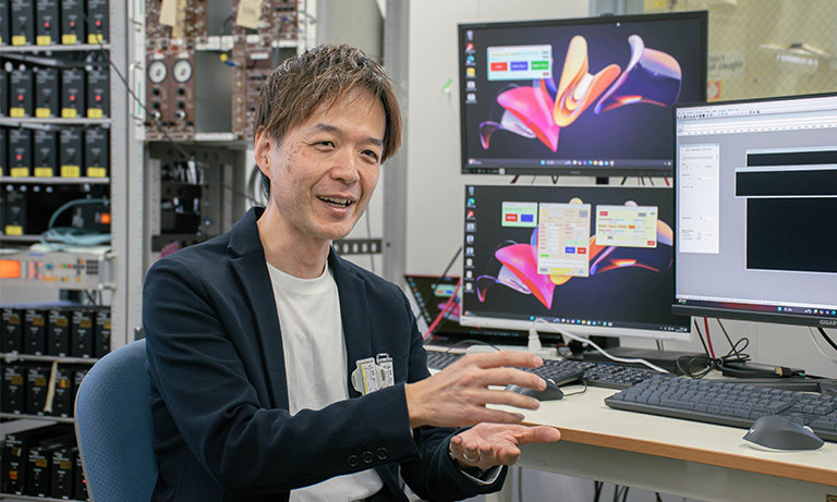
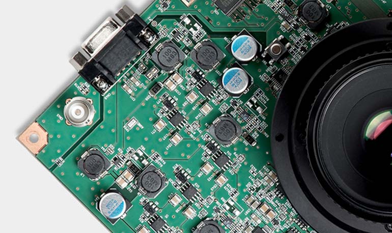
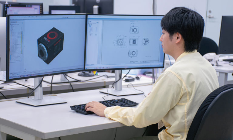
Hamamatsu Photonics develops cameras utilizing image sensor technologies such as sCMOS and TDI sensors. In addition, through more than 100 optical measurement simulations conducted annually, we have accumulated extensive expertise in optical measurement. Leveraging this experience and knowledge, we also apply our proprietary simulation engine to OEM camera development, enabling efficient selection of cameras optimized for specific customer applications.
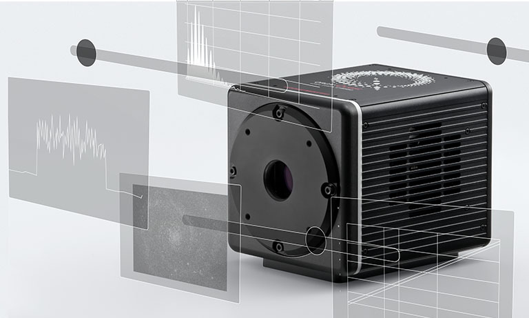
Selecting the most suitable image sensor technology is a key step in OEM camera development. For example, when imaging large-area objects, it is important to evaluate whether a tiling approach using two-dimensional sensors such as sCMOS, or a line-scan approach using a TDI sensor, will deliver better sensitivity and throughput under the customer’s actual operating conditions. However, these evaluations typically require significant time and cost to build test environments, and when multiple candidate approaches are available, there is a risk that prototype development may also proceed before the optimal imaging method has been definitively identified. Using our simulation engine, sensitivity and throughput can be modeled for scenarios in which a customer’s target object is imaged with different sensor technologies, as shown in Figure 1. This reduces development time and cost while supporting informed selection of the most appropriate image sensor technology.
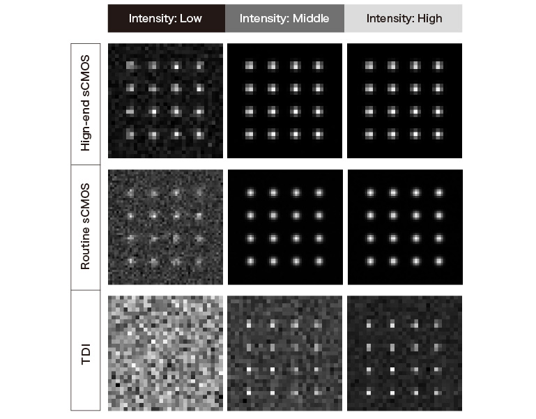
Fig. 1: Image simulation of sensitivity and throughput across primary sensors
Furthermore, even within the same image sensor technology, differences in characteristics such as quantum efficiency, pixel size, readout noise, and readout speed make the selection of an optimal sensor a time- and effort-intensive process. Our simulation engine supports comparisons within the same technology, contributing to the efficient narrowing down of image sensors best suited to specific customer applications. For example, in applications where sensitivity is a critical factor, the sensitivity performance of different image sensor technologies can be compared, as shown in Figure 2. In addition, if customers are already using third-party cameras, those cameras can be set as target specifications and included in comparative evaluations. For further details, please contact us.
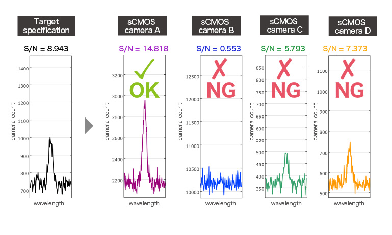
Fig. 2: Image simulation of sensitivity variations within the same sensor type
Experience a simple simulator on the web
Our Camera Simulation Lab* lets you try a simple web-based simulator. This tool allows you to view simulated images by selecting the sample type and imaging conditions.
* This tool differs from the actual simulation engine used in OEM camera development.
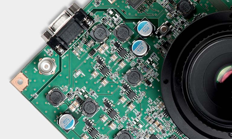
Thermal simulation available from early camera design stage
Based on customer requirements, we carry out camera enclosure design and thermal simulations of cooling mechanisms from the early stages of camera development. After assessing the customer’s operating environment and requirements, we incorporate analysis results, such as temperature distribution and thermal fluid behavior, into the mechanical design to optimize performance, cost, and camera size from the outset of OEM camera development.
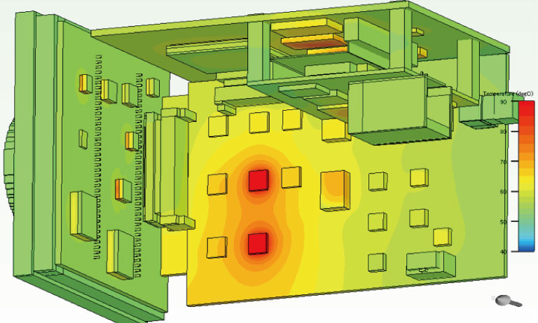
Fig. 3: Temperature distribution analysis
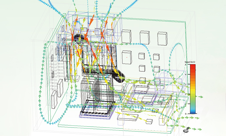
Fig. 4: Thermal fluid analysis
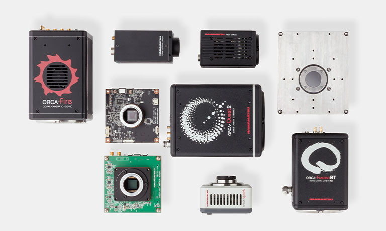
Related products
A routine camera with a back-illuminated sCMOS sensor. Although it is a routine model, it offers high sensitivity and resolution, as well as a wide field of view and low readout noise.
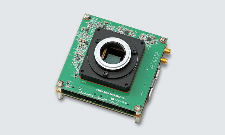
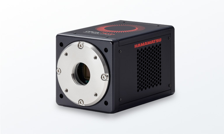
The C11440-52U30 is a camera equipped with a sCMOS image sensor based on the latest technology, achieving low noise, high resolution, and high-speed readout simultaneously. Its compact, OEM-ready board-level design makes it suitable for a wide range of applications, including embedded system integration.
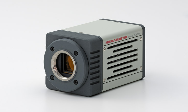
InGaAs cameras fill the gap between NIR wavelengths in the 950-1700 nm range, where silicon detectors are no longer sensitive. Our products capture images with QVGA to SXGA resolution and our extensive experience with InGaAs sensors allows us to offer cameras with exquisite image contrast and quality.
The C12849-111U is a high resolution and high sensitivity X-ray sCMOS camera. The camera's high resolution of 33 lp/mm makes it ideal for X-ray imaging of micro objects. Its compact size makes it suitable for embedding into systems such as micro X-ray CT systems.
TDI-CCD captures clear, bright images even in low-light conditions. In TDI mode, the CCD captures an image of a moving object while synchronously transferring integrated signal charges, greatly increasing sensitivity for high-speed imaging. Its back-thinned structure also delivers high quantum efficiency across a wide spectral range from UV to near IR (200 to 1100 nm).
Optical devices comprised of a bundle of micron-sized optical fibers. Used as an alternative of a lens to transmit light or an image with high efficiency and low distortion. Ideal when designing and building compact optical devices.

FOS fiber optic plates with a CsI scintillator feature an x-ray shield and low energy x-ray detection. Suitable for applications such as mammography, and medical and industrial imaging.
Fairchild Imaging is a semiconductor manufacturer specializing in high-performance CMOS image sensors for the visible to near-infrared and X-ray spectral ranges, and possesses advanced CMOS image sensor design technologies with exceptionally low-noise performance. With Fairchild Imaging becoming a member of the Hamamatsu Photonics Group, the combination of Fairchild Imaging’s technologies with Hamamatsu Photonics’ existing capabilities has established a framework that enables flexible responses to a broader range of customer requirements. By delivering products and solutions with greater added value than ever before, we will continue to contribute to our customers’ innovation.
![]()
- Confirmation
-
It looks like you're in the . If this is not your location, please select the correct region or country below.
You're headed to Hamamatsu Photonics website for GB (English). If you want to view an other country's site, the optimized information will be provided by selecting options below.
In order to use this website comfortably, we use cookies. For cookie details please see our cookie policy.
- Cookie Policy
-
This website or its third-party tools use cookies, which are necessary to its functioning and required to achieve the purposes illustrated in this cookie policy. By closing the cookie warning banner, scrolling the page, clicking a link or continuing to browse otherwise, you agree to the use of cookies.
Hamamatsu uses cookies in order to enhance your experience on our website and ensure that our website functions.
You can visit this page at any time to learn more about cookies, get the most up to date information on how we use cookies and manage your cookie settings. We will not use cookies for any purpose other than the ones stated, but please note that we reserve the right to update our cookies.
1. What are cookies?
For modern websites to work according to visitor’s expectations, they need to collect certain basic information about visitors. To do this, a site will create small text files which are placed on visitor’s devices (computer or mobile) - these files are known as cookies when you access a website. Cookies are used in order to make websites function and work efficiently. Cookies are uniquely assigned to each visitor and can only be read by a web server in the domain that issued the cookie to the visitor. Cookies cannot be used to run programs or deliver viruses to a visitor’s device.
Cookies do various jobs which make the visitor’s experience of the internet much smoother and more interactive. For instance, cookies are used to remember the visitor’s preferences on sites they visit often, to remember language preference and to help navigate between pages more efficiently. Much, though not all, of the data collected is anonymous, though some of it is designed to detect browsing patterns and approximate geographical location to improve the visitor experience.
Certain type of cookies may require the data subject’s consent before storing them on the computer.
2. What are the different types of cookies?
This website uses two types of cookies:
- First party cookies. For our website, the first party cookies are controlled and maintained by Hamamatsu. No other parties have access to these cookies.
- Third party cookies. These cookies are implemented by organizations outside Hamamatsu. We do not have access to the data in these cookies, but we use these cookies to improve the overall website experience.
3. How do we use cookies?
This website uses cookies for following purposes:
- Certain cookies are necessary for our website to function. These are strictly necessary cookies and are required to enable website access, support navigation or provide relevant content. These cookies direct you to the correct region or country, and support security and ecommerce. Strictly necessary cookies also enforce your privacy preferences. Without these strictly necessary cookies, much of our website will not function.
- Analytics cookies are used to track website usage. This data enables us to improve our website usability, performance and website administration. In our analytics cookies, we do not store any personal identifying information.
- Functionality cookies. These are used to recognize you when you return to our website. This enables us to personalize our content for you, greet you by name and remember your preferences (for example, your choice of language or region).
- These cookies record your visit to our website, the pages you have visited and the links you have followed. We will use this information to make our website and the advertising displayed on it more relevant to your interests. We may also share this information with third parties for this purpose.
Cookies help us help you. Through the use of cookies, we learn what is important to our visitors and we develop and enhance website content and functionality to support your experience. Much of our website can be accessed if cookies are disabled, however certain website functions may not work. And, we believe your current and future visits will be enhanced if cookies are enabled.
4. Which cookies do we use?
There are two ways to manage cookie preferences.
- You can set your cookie preferences on your device or in your browser.
- You can set your cookie preferences at the website level.
If you don’t want to receive cookies, you can modify your browser so that it notifies you when cookies are sent to it or you can refuse cookies altogether. You can also delete cookies that have already been set.
If you wish to restrict or block web browser cookies which are set on your device then you can do this through your browser settings; the Help function within your browser should tell you how. Alternatively, you may wish to visit www.aboutcookies.org, which contains comprehensive information on how to do this on a wide variety of desktop browsers.
5. What are Internet tags and how do we use them with cookies?
Occasionally, we may use internet tags (also known as action tags, single-pixel GIFs, clear GIFs, invisible GIFs and 1-by-1 GIFs) at this site and may deploy these tags/cookies through a third-party advertising partner or a web analytical service partner which may be located and store the respective information (including your IP-address) in a foreign country. These tags/cookies are placed on both online advertisements that bring users to this site and on different pages of this site. We use this technology to measure the visitors' responses to our sites and the effectiveness of our advertising campaigns (including how many times a page is opened and which information is consulted) as well as to evaluate your use of this website. The third-party partner or the web analytical service partner may be able to collect data about visitors to our and other sites because of these internet tags/cookies, may compose reports regarding the website’s activity for us and may provide further services which are related to the use of the website and the internet. They may provide such information to other parties if there is a legal requirement that they do so, or if they hire the other parties to process information on their behalf.
If you would like more information about web tags and cookies associated with on-line advertising or to opt-out of third-party collection of this information, please visit the Network Advertising Initiative website http://www.networkadvertising.org.
6. Analytics and Advertisement Cookies
We use third-party cookies (such as Google Analytics) to track visitors on our website, to get reports about how visitors use the website and to inform, optimize and serve ads based on someone's past visits to our website.
You may opt-out of Google Analytics cookies by the websites provided by Google:
https://tools.google.com/dlpage/gaoptout?hl=en
As provided in this Privacy Policy (Article 5), you can learn more about opt-out cookies by the website provided by Network Advertising Initiative:
http://www.networkadvertising.org
We inform you that in such case you will not be able to wholly use all functions of our website.
Close